Timing diagram
for operations of AND gate
Visualize the operations of an AND gate with our comprehensive timing diagram template.
- Templates
- Timing diagram templates
- Timing diagram for operations of AND gate
About the timing diagram example
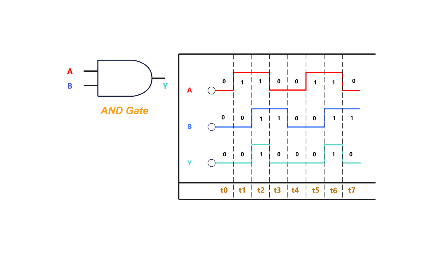
The template provides a clear and detailed visual representation of the behaviour of an AND gate in digital circuits. It includes key input signals (A and B) and the resulting output signal (Y).
The template demonstrates how the output changes in response to different combinations of input signals over time. Each transition is chronologically organized, showing the precise moments when the output goes high or low based on the input conditions, thereby ensuring a clear understanding of the gate's operation.
How to use the timing diagram template
Click the provided link and select "Edit Online" to open the template in the Edraw Online editor.
Modify input signals (A and B) and the output signal (Y) to fit your AND gate scenario.
Adjust the timing and sequence of inputs to match the AND gate's operation, modifying labels and lines as needed.
Ensure all transitions and timings are accurate and clear, making any necessary adjustments.
Export your completed diagram in SVG, PPTX, PDF, or JPG format for sharing or integration into other documents.
Why one should use the timing diagram template?
Using this template provides a structured way to visualize and understand the timing and sequence of events in digital circuits involving AND gates. It helps in breaking down complex logical operations into clear, manageable steps, facilitating better communication among team members and stakeholders.
This template enhances circuit design accuracy, aids in identifying potential issues, and ensures all aspects of the gate's operation are accounted for. By using this template, organizations can streamline the documentation process, improve clarity, and support effective circuit analysis and development.
FAQs about the timing diagram for operations of AND gate
-
What is a timing diagram in the context of an AND gate?
A timing diagram in the context of an AND gate illustrates the chronological sequence of input signals and the corresponding output signal, showing how the output changes in response to different input combinations over time.
-
How detailed should a timing diagram for an AND gate be?
The diagram should be detailed enough to cover all essential input and output transitions, but not overly complex. It should clearly depict the timing and logical flow to ensure comprehensibility.
-
Can this timing diagram template be customized for different types of logic gates?
Yes, the template can be customized to fit various types of logic gates, such as OR gates, NOT gates, and NAND gates, by adjusting the input and output signals accordingly.
-
What are common pitfalls to avoid when creating a timing diagram for an AND gate?
Common pitfalls include overcomplicating the diagram with too much detail, omitting key transitions, and not validating the diagram with relevant stakeholders. Ensuring simplicity, completeness, and stakeholder review can help avoid these issues.
-
How can a timing diagram help in improving digital circuit design?
A timing diagram helps improve digital circuit design by providing a clear visual representation of the sequence and timing of signal transitions. It aids in identifying potential issues, ensuring all processes are accounted for, and facilitating better communication among team members.
Related templates

Get started with EdrawMax today
Create 210 types of diagrams online for free.
Free Download Free Download Draw a diagram free Draw a diagram free Draw a diagram free