- Templates
- Circuit diagram templates
- 555 timer IC circuit diagram
About this 555 timer IC circuit diagram
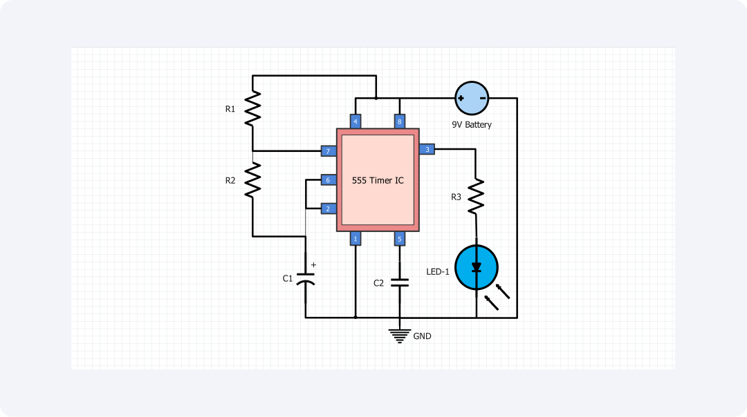
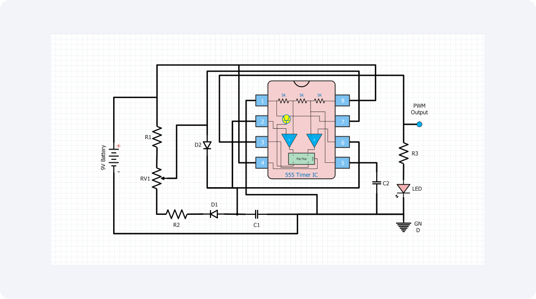
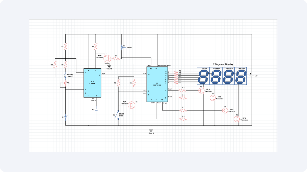
The 555 timer is an integrated circuit which is one of the most flexible devices that exist in the electronics field. This circuit diagram demonstrates one of its most common configurations: a simple astable oscillator.
The following components make the circuit; a 555 timer, two resistors, and a capacitor. When power is applied the capacitor begins to charge through the resistors R1 & R2. Once the voltage across the capacitor has risen to 2/3rd of the supply voltage the trigger input of the 555 timer is triggered.
The output goes high. The capacitor then discharges through R2. When the switch S1 is opened, the capacitor is charged to the battery's voltage.
When the voltage across the capacitor comes down to 1/3 rd of the voltage of the supply, the threshold input level of the 555-timer is triggered and the output switches to a low state. The results repeat in this fashion producing a square wave.
The astable oscillator configuration of the 555-timer is very versatile and can be used as a frequency generator, and pulse generator, for blinking LEDs, to produce sound signals, and for controlling motors.
With proper experiment and adjustment of the resistor and capacitor values, you can control the frequency and duty cycle of a waveform. Due to this flexibility, all sorts of electronic projects find the 555-timer useful in the project.
This circuit diagram can be of great help to anyone interested in learning more about this 555 timer IC or anyone who wishes to design a simple circuit using this chip. The diagram is clear and uncluttered, and the components used in the construction of the diagram are easily obtainable.
Related templates
Get started with EdrawMax today
Create 210 types of diagrams online for free.
Draw a diagram free Draw a diagram free Draw a diagram free Draw a diagram free Draw a diagram free
