


A Field-Programmable Gate Array (FPGA) is a reconfigurable hardware chip designed for multitasking. Its programming can be updated and reconfigured based on user requirements, enabling it to perform a wide variety of tasks efficiently.
In this guide, we are going to explore
- What is an FPGA
- How does it work
- How to draw a block diagram for an FPGA
- What are the applications of an FPGA
In the end, you will understand how FPGAs can be configured to perform different tasks without altering the underlying hardware of a single chip. You will also learn how to create an FPGA block diagram, which provides valuable insights into the internal structure of an FPGA and enhances your understanding of its functionality.
In this article
FPGA Block Diagram and Its Working Principle
An FPGA block diagram discusses the main components used in the system, and it could be the best tool to identify the system's working and a pathway for the researchers and developers to create better devices in the future. Let’s check out the block diagram of an FPGA.
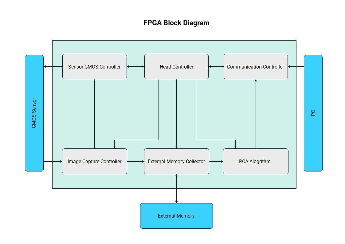
Here are a few of the main components used in an FPGA.
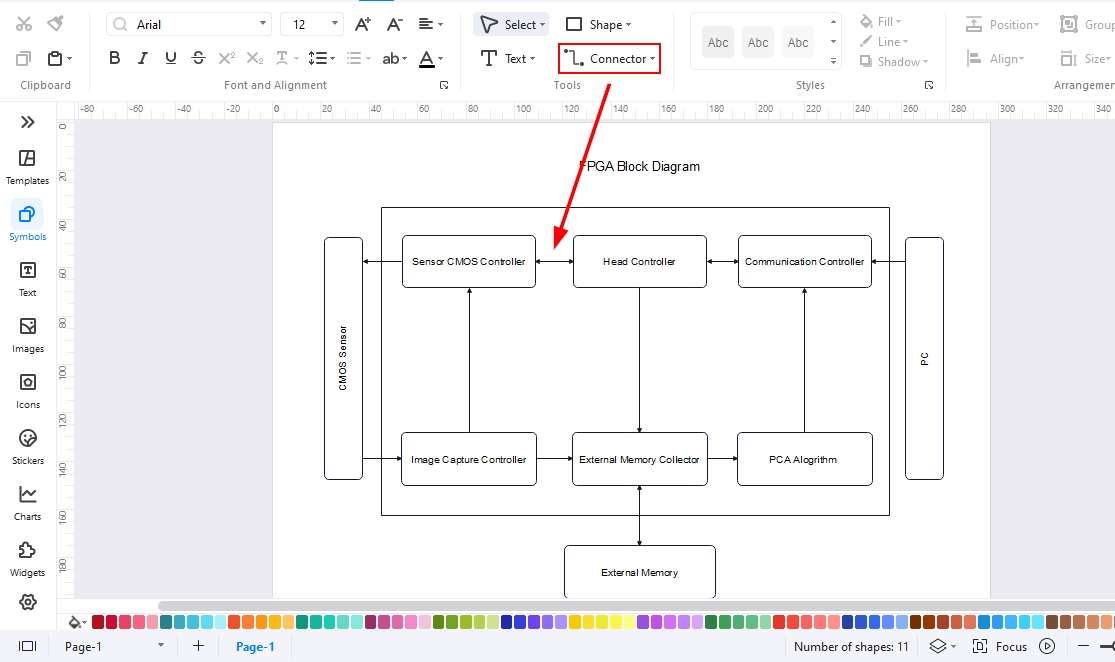
- Head Controller: It is known as the central control unit in an FPGA. The duty of the head controller is to manage input/output operations and create a path for a proper data exchange channel among the subsystems in the FPGA.
- Memory Controller: The memory controller in the FPGA is connected with the external memory disks, including RAM/ROM or hard drives. It controls the data sharing between the external and internal memory compartments in the FPGA.
- CMOS Controller: The analogue signal is checked and converted to a digital signal through the CMOS Controller. It manages the interface between the Sensor and the FPGA. These sensors are responsible for creating images and controlling all sensor-based systems through the CMOS Controller.
- PCA Algorithm: It is not a hardware in an FPGA, but an Algorithm that is implemented on the FPGA for specified tasks. It is mostly used in image processing and data reduction systems. It manages hundreds of matrix calculations in milliseconds to provide recognizable real-time data.
Now, let's check out how the FPGA as a whole works.
The head controller initializes the whole operation by collecting the data from the external memory attached to the FPGA. The inputs are received from these memory chips, which are attached.
The CMOS controller sends the signals to the system, and it is responsible for the digitization of these signals.
Now, this data is transmitted and processed through the communication controller. The PCA algorithm then uses logic blocks to convert this data into the required form. It is vital for the feature extraction and dimensionality reduction in the system.
Applications of FPGA
An FPGA (Field-Programmable Gate Array) is a versatile and reprogrammable semiconductor device that allows developers to customize hardware based on specific requirements.
Unlike ASICs, which are fixed-function circuits, FPGAs can be reconfigured to perform different tasks as needed. Their combination of high performance and reliability makes them valuable across a wide range of applications.
Below are some of the key uses of FPGAs.
Networking and Telecommunication Industry
FPGAs are mostly used in network and telecommunications systems due to their signal processing abilities. The 3G, 4G, and 5G technologies use these devices for proper data transmission and help them in protocol implementation and packet switching. High-speed base stations and network towers use this technology to send data quickly.
Radar Systems
FPGAs are used in most radar systems, satellite communications, and guidance systems. The quick data processing and reliability of these systems are crucial during warfare.
The ADAS systems use these devices, helping pilots track the flight path and supporting them while engaging the target jet as well.
Medical and Healthcare
FPGAs offer low latency, enabling healthcare providers to analyze scans and diagnose a disease. Faster image processing and real-time monitoring help doctors diagnose and perform surgeries.
Most of the time, they are used in MRI scanners, CT scan machines, and portable medical equipment like ECG machines.
Cloud Computing
Data centers are using these devices to accelerate and save a large amount of data in real time. They are being used in AI and deep learning systems to process data quickly. The reconfiguration ability of these devices helps developers handle parallel tasks like data encryption, compression, and CPU load reduction.
How to Create an FPGA Block Diagram
Block diagrams are widely used to simplify complex models, making them easier to understand. In the case of FPGAs, a block diagram illustrates the fundamental concepts of their operation, serving as a valuable resource for students, engineers, and researchers alike. But how do you start creating such diagrams? The key lies in using a specialized tool that provides extensive customization options.
EdrawMax, one of the leading diagramming tools, makes it easy to design detailed and accurate FPGA block diagrams. Let’s explore some of its standout features.
- User-Friendly Interface: EdrawMax comes with a clean interface that even suits beginners. It provides a clean interface, drag and drop functionality, image addition, text formats, and much more.
- Huge Symbols Library: EdrawMax's Symbol library is vast, providing all the symbols, elements, and text formats you need to complete your block diagram.
- Customization Tools: EdrawMax is full of tools that offer different color schemes you need for your blocks, text formats, and themes. It provides connector tools to add relationships among the blocks.
- Templates Library: EdrawMax offers templates for each category, helping you complete your own design through these templates. You can use a template as it is if it fulfils your demands.
- Multiple Import and Export Options: EdrawMax is helpful for a wide audience, enabling them to import and export their block diagrams in different formats. You can import Visio files and directly edit them.
Now, let's check out how to create an FPGA Block diagram with the help of EdrawMax using different methods.
Method 1: Make a FPGA block diagram from scratch
Starting a design from scratch can feel daunting, but with a specialized tool like EdrawMax, the process becomes much easier. It offers all the essential symbols, tools, and customization options you need to create a complete and professional block diagram. Follow the steps below to design your diagram from the ground up.
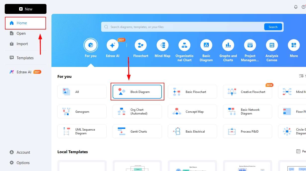
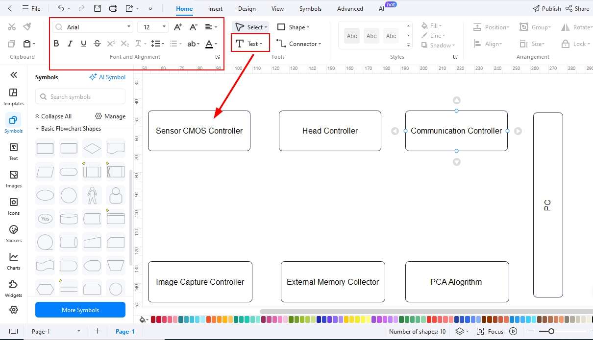
Step1 Open EdrawMax and get started
- Open EdrawMax and click New on the tool's home page, or find the block diagram section to open the empty canvas.
- Once the empty canvas is opened, you will find the relevant elements.
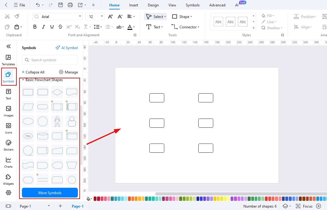
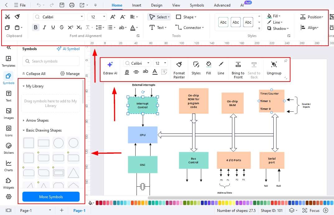
Step2 Drag and Drop Symbols and Elements on the canvas
- Click the Symbols library and find the most suitable elements for your design.
- Click an element or drag it directly to the canvas.
Step3 Add Text for each Block
- Arrange the elements in the order you need them to be.
- Double-click the block to add text for each block.
Step4 Add Relationships/ Connections
- Use the connector tool to add a relationship.
- If you need arrows, you can also use the symbols library to find arrows of different shapes.
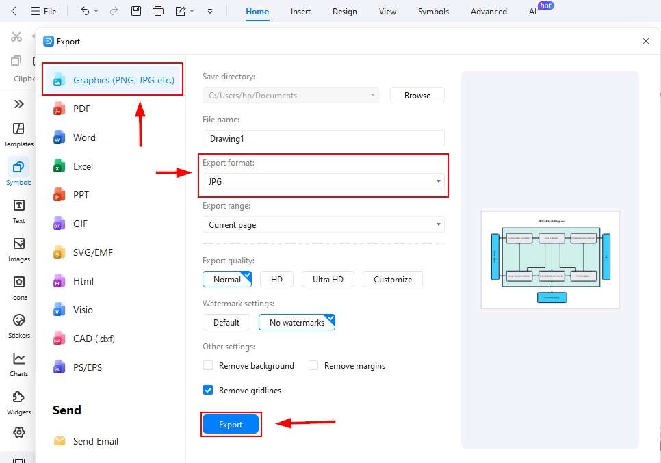
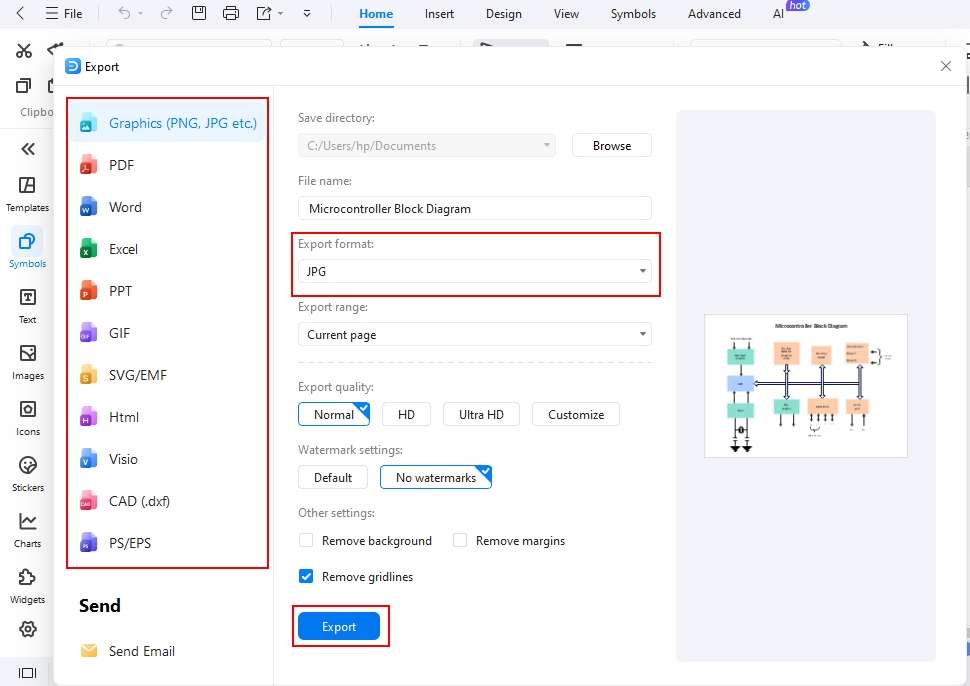
Step5 Export your Block Diagram
- After all the editing, it’s time to export your block diagram.
- Click the export button or file in the upper left corner of the screen and choose a format. Set all your preferences and click export to save the design.
Method 2: Use a FPGA block diagram template
EdrawMax, a leading diagramming tool, provides a comprehensive template library to help you get started quickly. These ready-made templates require only minor edits to create a custom design, saving you time while delivering professional results. Follow the step-by-step guide below to produce polished diagrams fast.
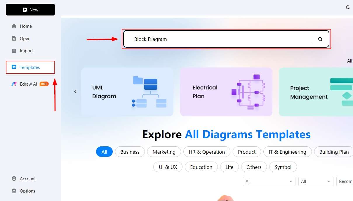
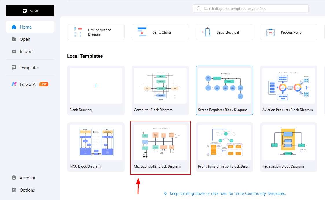
Step1 Open Templates Library
- Open EdrawMax Home Page and click templates on the left-hand side of the screen.
- Search for the block diagram templates available in the library using the search bar.
Step2 Select a Template and Click it
- Start looking for the template that is closest to your block diagram.
- Click it to bring it onto the canvas and start further editing.
Step3 Edit the template
- Start editing the template on the canvas.
- Now, add or delete any shape needed. Use your own text to make your own block diagrams.
- You can change colours and themes for your block diagram here.
Step4 Export your file
- After all the edits, you need to export your design.
- Click the file and find the export option available, or use the export button available at the top of the menu bar and select a format to save it.
Final Thoughts
The programmability of FPGAs gives developers the flexibility to use them for multitasking, as they can handle many processes independently and significantly reduce the workload on the CPU.
An FPGA block diagram illustrates the fundamental concepts and components of the device, making it easier to understand its structure and operation. Such diagrams are essential for developers, who often rely on them to plan future modifications and maximize performance.
With EdrawMax, you can easily create professional FPGA block diagrams that simplify complex systems and make them more accessible to your audience.
AI Diagram Generator
Enter your prompt. Upload files if needed. Generate diagrams, charts, or slides instantly.