


The flash memory circuit is one of the easiest examples of a data storage system. It shows how controllers, connectors, and memory ICs interact in an endless manner to control the stream of data and information storage.
Flash memory is predominant in modern devices since it is quick in data transfer, consumes less power, and is small. It comes in USB drives, SD cards, and various embedded systems.
In this article, you will learn the principles of working of flash memory, its major components, and how they are used. We will also show how you can make your own flash memory circuit diagram using EdrawMax, beginning with a drawing and ending with the styling and export.
In this article
What is a Flash Memory Storage Circuits
A flash memory circuit is a storage system that stores and retrieves data and does not require any moving parts. It links a flash memory and a controller chip to store data in an off state.
A computer or camera controller transmits/receives data via a USB or SD connection. It controls the location of data in the flash memory cells. Control signals, data lines, and power lines assist in the movement of data between the host device and the storage chip.
These are miniature circuits that are energy-efficient. They are applied to USB drives, SD cards, and most portable or built-in devices that effectively require the storage of data.
Key Components in a Flash Memory Diagram
The digital logic system and control lines in a flash memory circuit enable efficient data transfer and storage operations. The system components function independently to perform data exchange, power distribution, and information storage tasks.
Connector (USB or SD Slot)
The connector functions as the connection point that links external devices to the controller unit. The connector enables data transfer, clock signal exchange, and power signal transmission for successful read/write operations.

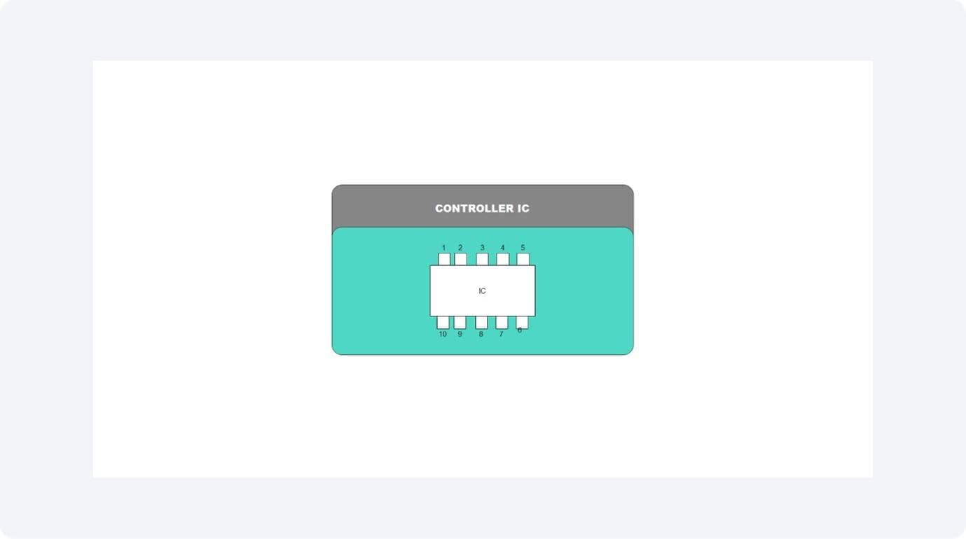
Controller IC
The controller functions as the main control center of the system. The controller accepts data instructions, executes communication protocols, and maintains contact with flash memory storage. The controller manages data transfer schedules, performs error detection and correction functions, and controls LED status indicators.
Flash Memory IC
Data is permanently stored in this non-volatile storage component. It uses a data bus and control lines to communicate with the controller while storing data in memory cells arranged into blocks.

Power Source (3.3 V / 5 V)
The system needs a constant DC power supply that operates at 5 volts for USB drives and 3.3 volts for SD cards. The power line supports both controller and memory operations while ensuring proper logic-level operation.

Working Principle Explained
The flash memory circuit is activated when the connector (USB or SD slot) receives a signal from the host. These cables have power and data. The USB or SD interface provides the data to the controller chip, which then converts it into commands by which data is directed to and out of the flash memory chip.
The controller within the system takes care of address mapping, corrects data errors, and writes cycles to ensure that the storage is reliable. The device has an LED light that is activated when the device begins operating to indicate that it is in operation. Power management maintains a constant voltage of 5 V USB, 3.3 V SD to avoid corruption of data.
The flash memory and the controller are complementary to each other and enable quick, reliable, and rewritable data storage on contemporary electronic gadgets.
Continuous vs. Intermittent Operation
Continuous Operation: When the device is actively transferring data, the controller and flash memory remain in constant communication. The power and data lines maintain their active state to provide stable high-speed operation.
Intermittent Operation: The controller enters low-power mode when data transfer stops or the device becomes inactive, but it keeps all stored information safe. This reduces energy use and heat generation in portable devices.
Role of Controller Timing
The controller determines data access timing through its precise timing signals, which control when and how data is read or written. The controller and flash memory need to operate in sync because this synchronization protects data from damage and allows for quick access to stored information.
Flash Memory Circuit Diagram Examples
Flash memory circuits differ slightly in configuration depending on the interface type and voltage level. Both designs share similar control logic but vary in connectors and power management. Below are two common examples of how flash memory is implemented in portable devices.
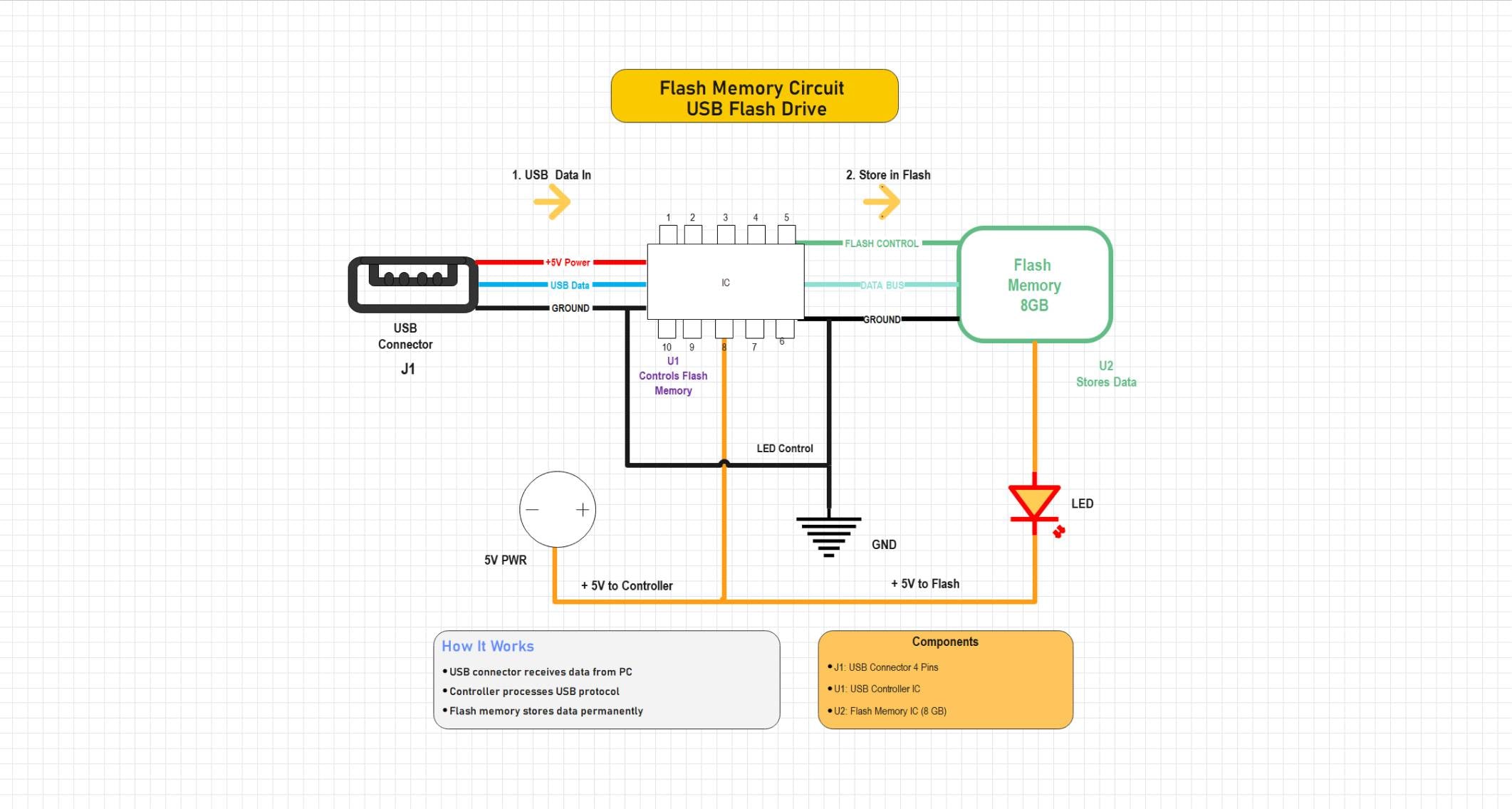
Example 1: Flash Memory Circuit — USB Flash Drive
This system depicts USB flash drives. The USB connector is connected to the controller IC that supplies power and data to the device, as well as controlling communication with the flash memory chip. The system is also displayed by the LED, indicating system operation, and there is light output when reading and writing. The gadget uses 5 V of power to offer easy storage of data in the form of a plug-and-play component that is used in computers and embedded systems.
This circuit demonstrates a USB flash drive system where a USB controller manages data transfer between the USB connector and flash memory. The controller interprets USB protocol commands and directs data storage operations within the flash memory. A 5V supply powers both the controller and memory, while an LED indicator signals data activity. The design illustrates the core functional blocks of USB-based flash storage devices used in portable data storage applications.
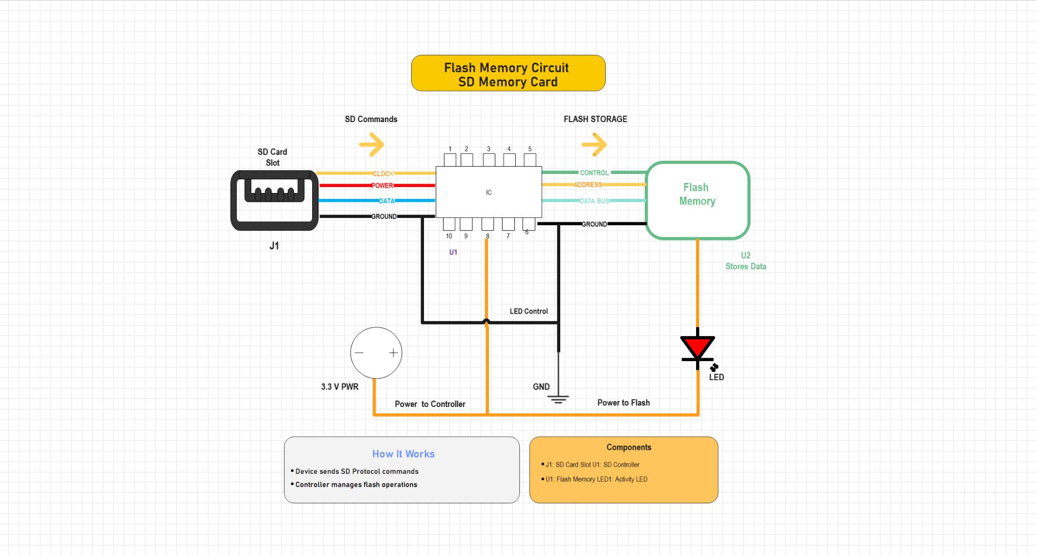
Example 2: Flash Memory Circuit — SD Memory Card
This circuit demonstrates the operation of an SD card. The SD slot sends clock and data signals to the SD controller, which manages flash storage operations. It runs at 3.3 V and uses similar logic to the USB version, but optimized for portable devices like cameras and smartphones. The LED indicates activity during data transfer.
This circuit illustrates an SD memory card interface where an SD controller manages communication between the SD card slot and flash memory. The controller processes SD protocol commands and controls data transfer through address, control, and data lines. A 3.3V power supply feeds both the controller and flash module, while an LED indicator displays flash activity. The design demonstrates the basic operation of SD-based flash storage systems used in embedded and digital devices. //
How to Draw a Flash Memory Storage Circuit Diagram in EdrawMax
Designing a flash memory storage circuit is straightforward with EdrawMax. Its drag-and-drop interface and ready-to-use electronic components let you quickly assemble USB or SD memory circuits with controllers, flash modules, and power connections. You can easily visualize data flow, customize layouts, and export professional schematics within minutes. Take all of these steps.
Step1 Initiate a New Project
- Open EdrawMax.
- Click New on the left panel.
- Select Blank Drawing to begin with a blank canvas.

Step2 Select Electronic Symbol Libraries
- Select the left toolbar of Symbols or More Symbols.
- Right-click Manage and then Add More Symbols.
- Add the Electrical or Circuit and Logic libraries to use such components as MOSFETs, diodes, inductors, and capacitors.

Step3 Add the Controller IC, USB Connector, Flash Memory, and Source
- Place a power source and a ground.
- Add a controller IC, a USB connector for connection purposes, and flash memory for storage.

Step4 Complete the Wiring
- Use the connector tool to complete the wiring.
- Be cautious about the inputs and outputs of the controller IC and connect them to the corresponding terminals.

Step5 Label and Write Description
- Name the parts (e.g., controller IC, flash memory, etc).
- Change the colours of the desired element.
- Write a description or explanation for better understanding.

Step6 Export Your Created Diagram
- Finalise the diagram by checking the alignments and spacing to be clear.
- After that, save your design.
- The tool allows users to save their diagrams in PNG, PDF, and SVG file formats.

Create a Circuit Diagram Online Now
EdrawMax makes it easy to design flash memory circuits within minutes. Its drag-and-drop tools and ready-made electronic symbols, like controllers, flash chips, and connectors, allow you to create clear, professional diagrams with ease. You can customize, format, and export your designs quickly for reports or presentations.
Key Features
- The software includes built-in symbol libraries that support controllers, connectors, memory ICs, and LEDs.
- The platform offers an easy-to-use drag-and-drop editor that includes smart connectors for simple operations.
- The system enables users to work together in real time while providing protection.
- The system's pre-designed templates allow users to quickly develop circuits.
- The tool allows users to save their diagrams in PNG, PDF, and SVG file formats.
Best Practices for Creating Accurate Designs
The design of a flash memory circuit needs proper implementation to achieve fast data transfer operations and maintain reliable information storage capabilities. The following are some of the tips that you should follow to have a reliable and safe circuit:
Use Appropriate Power Levels
It is important to always ensure that you supply the right voltage depending on the type of circuit: 5 V on USB flash disks and 3.3 V on SD memory cards. The controller and flash IC will be damaged permanently once the supply voltage is above the safe limits, but their read/write functions will begin to become unstable once the supply voltage falls below their suggested operating limits.
Ensure Clean Signal Routing
The data and clock lines need to remain brief while receiving proper grounding to reduce both noise and crosstalk interference. Use separate traces for power and signal paths where possible and include decoupling capacitors near ICs to maintain signal integrity.
Include LED indicators
Add LED indicators to show active data transfer or standby states. The system provides user feedback while tracking controller operations for testing and troubleshooting purposes.
Maintain ESD and Surge Protection
The design should include ESD protection diodes, series resistors, and TVS diodes, which should be placed near the connector pins to protect against static discharge and voltage spikes. Proper grounding and shielding ensure the reliability and longevity of the flash memory circuit.
Conclusion
A flash memory circuit diagram is a great resource for learning how contemporary storage devices operate. The system shows how the connector works with the power supply and controller to permanently store data in flash memory. With EdrawMax, users can quickly and expertly create their own USB or SD flash memory diagrams. The platform's user-friendly interface, which supports multiple symbols for users without advanced knowledge, allows users to create circuits.
AI Diagram Generator
Enter your prompt. Upload files if needed. Generate diagrams, charts, or slides instantly.